
It has been a long time that I posted on my webpage related to Digital Design and SoC concepts. This post will be related to Zynq Processing System (PS) DMA usage example and performance analysis on data transfer between DDR3 RAM, OCM and PL Block RAM. I will provide both PL and PS designs and source codes through my github page.
If you are already using or plan to use Zynq SoC, it is very likely that you are going to need some kind of data transfer between different memory locations of the SoC. If you rely on CPU load/store instructions to move data between memory locations, it would be a waste of precious CPU time that should be utilized for arithmetic and logical operations or decision making which are core operations for any problem. Direct memory access (DMA) is a well-known method to take the burden of data moving from CPU to DMA engine. In DMA, CPU only programs DMA engine for configuration such as how much data will be transferred, where are the source and destination addresses etc. and then the DMA engine handles data transfer and inform CPU that the transfer is done.
Before starting the details of the topic and implementations, I want to refer anyone who is interested in data transfer methods between PS and PL in system design perspective to read the document below:
https://docs.xilinx.com/v/u/en-US/wp459-data-mover-IP-zynq
One of the peripherals in the PS is the DMAC (DMA controller) engine:
In Zynq Technical Reference Manual (TRM) Chapter 9 is related to this peripheral. The DMAC peripheral is defined in that document as:
“The DMA controller (DMAC) uses a 64-bit AXI master interface operating at the CPU_2x clock rate to
perform DMA data transfers to/from system memories and PL peripherals. The transfers are
controlled by the DMA instruction execution engine. The DMA engine runs on a small instruction set
that provides a flexible method of specifying DMA transfers. This method provides greater flexibility
than the capabilities of DMA controller methods”
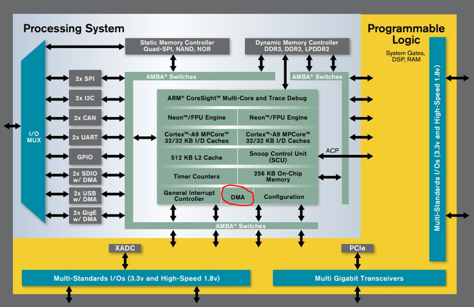
The connectivity diagram for the PS DMAC is given as:

From the figure it is understood that PS DMAC has access to 265K On-Chip Memory, from AXI Master interface to the PL and DDR memory controller. I wanted to utilize all of the connections, so that designed a system architecture as below:

So I tested data transfers latency times for 4 different scenarios:
1) From DDR to DDR with PS DMA
2) From DDR to OCM with PS DMA
3) From DDR to PL BRAM with PS DMA 4) From DDR to DDR with CPU load/store instructions
4) From DDR to DDR with CPU load/store instructions
I first created a blok design in VIVADO. I only added a block RAM controller and a 32K BRAM:

I have Avnet Zedboard, the utilization is as below:

You can regenerate the block design with tcl scripts that I provided in my github page:
https://github.com/mbaykenar/zynq-soc-hw-sw-design/blob/main/ders14/zynq_psdma.tcl
https://github.com/mbaykenar/zynq-soc-hw-sw-design/blob/main/ders14/system.tcl
Then I exported the design to Vitis and started SW design. First some constant definitions:
#define DMA_TRANSFER_SIZE 32768
// INTC
#define INTC_DEVICE_ID XPAR_SCUGIC_0_DEVICE_ID
#define INTC_BASEADDR XPAR_PS7_SCUGIC_0_BASEADDR

// DMA
#define DMA0_ID XPAR_XDMAPS_1_DEVICE_ID
The instances for the interrupt controller and DMA peripheral:
// driver instances
static XScuGic Intc; // The instance of the generic interrupt controller (GIC)
XDmaPs Dma;				/* PS DMA */
I created byte arrays for the source and destination. I needed to do some trick on definition of arrays such that where the arrays will reside? In OCM, PL BRAM or DDR? In order to do this, I first edited linker script and created 2 different sections first for OCM and second for BRAM. Notice that DDR is already defined in linker script. In order to create sections I added mba_ocm_section and mba_bram_section before the text section in the linker code:
SECTIONS
	{
	.mba_ocm_section : {
	    KEEP(*(.mba_ocm_section))
	} > ps7_ram_1


	.mba_bram_section : {
	    KEEP(*(.mba_bram_section))
	} > axi_bram_ctrl_0_Mem0


	.text : {
	   KEEP (*(.vectors))
	   *(.boot)
	   *(.text)
	   *(.text.*)
	   *(.gnu.linkonce.t.*)
	   *(.plt)
	   *(.gnu_warning)
	   *(.gcc_execpt_table)
	   *(.glue_7)
	   *(.glue_7t)
	   *(.vfp11_veneer)
	   *(.ARM.extab)
	   *(.gnu.linkonce.armextab.*)
	} > ps7_ddr_0
You can find edited linker script in my github page:
https://github.com/mbaykenar/zynq-soc-hw-sw-design/blob/main/ders14/lscript.ld
So after modifying linker script I created arrays in C code as:
// Source and Destination memory segments
unsigned char Src[DMA_TRANSFER_SIZE];
unsigned char Dst_DDR[DMA_TRANSFER_SIZE];
unsigned char Dst_OCM[DMA_TRANSFER_SIZE]__attribute__((section(".mba_ocm_section")));
unsigned char Dst_BRAM[DMA_TRANSFER_SIZE]__attribute__((section(".mba_bram_section")));
With these, Dst_OCM array will reside in OCM and Dst_BRAM will resides at PL BRAM.
After basic configuration and initialization settings in the main function, I first transfer data from DDR to DDR by utilizing PS DMAC and measure the latency with the code below:
	/******************************************************************************/
	// First transfer DDR to DDR with PS DMA
	/******************************************************************************/
	DmaCmd.BD.SrcAddr = (u32)Src;
	DmaCmd.BD.DstAddr = (u32)Dst_DDR;
	DmaCmd.BD.Length =  DMA_TRANSFER_SIZE;

	// initialize writedata array with random numbers
    int i = 0;
    for (i=0;i<DMA_TRANSFER_SIZE;i++)
    {
    	Src[i] = lfsr_rand();
    }

    // clear destination array
    for (i=0;i<DMA_TRANSFER_SIZE;i++)
    {
    	Dst_DDR[i] = 0x00;
    }

	Done = 0;
	Status = XDmaPs_Start(&Dma, Channel, &DmaCmd, 0);
	XTime_GetTime(&tStart);
	if (Status == XST_SUCCESS)
	{
		while (Done == 0);
	}
	XTime_GetTime(&tEnd);

	u64 et_dma_ddr = tEnd - tStart;
	float et_us_dma_ddr = ((float)((float)et_dma_ddr) / 333333333.3)*1000000;

    // check if write and read arrays are equal
    for (i=0;i<DMA_TRANSFER_SIZE;i++)
    {
    	if (Src[i] != Dst_DDR[i])
    	return XST_FAILURE;
    }
The second transfer is from DDR to OCM:
	/******************************************************************************/
	// Second transfer DDR to OCM with PS DMA
	/******************************************************************************/
	DmaCmd.BD.SrcAddr = (u32)Src;
	DmaCmd.BD.DstAddr = (u32)Dst_OCM;

    // refill source array with pseudo-random numbers
    for (i=0;i<DMA_TRANSFER_SIZE;i++)
    {
    	Src[i] = lfsr_rand();
    }

    // clear destination array
    for (i=0;i<DMA_TRANSFER_SIZE;i++)
    {
    	Dst_OCM[i] = 0x00;
    }

	Done = 0;
	Status = XDmaPs_Start(&Dma, Channel, &DmaCmd, 0);
	XTime_GetTime(&tStart);
	if (Status == XST_SUCCESS)
	{
		while (Done == 0);
	}
	XTime_GetTime(&tEnd);

	u64 et_dma_ocm = tEnd - tStart;
	float et_us_dma_ocm = ((float)((float)et_dma_ocm) / 333333333.3)*1000000;

    // check if write and read arrays are equal
    for (i=0;i<DMA_TRANSFER_SIZE;i++)
    {
    	if (Src[i] != Dst_OCM[i])
    	return XST_FAILURE;
    }
The third is from DDR to BRAM:
	/******************************************************************************/
	// Third transfer DDR to BRAM with PS DMA
	/******************************************************************************/
	DmaCmd.BD.SrcAddr = (u32)Src;
	DmaCmd.BD.DstAddr = (u32)Dst_BRAM;

    // refill source array with pseudo-random numbers
    for (i=0;i<DMA_TRANSFER_SIZE;i++)
    {
    	Src[i] = lfsr_rand();
    }

    // clear destination array
    for (i=0;i<DMA_TRANSFER_SIZE;i++)
    {
    	Dst_BRAM[i] = 0x00;
    }

	Done = 0;
	Status = XDmaPs_Start(&Dma, Channel, &DmaCmd, 0);
	XTime_GetTime(&tStart);
	if (Status == XST_SUCCESS)
	{
		while (Done == 0);
	}
	XTime_GetTime(&tEnd);

	u64 et_dma_bram = tEnd - tStart;
	float et_us_dma_bram = ((float)((float)et_dma_bram) / 333333333.3)*1000000;

    // check if write and read arrays are equal
    for (i=0;i<DMA_TRANSFER_SIZE;i++)
    {
    	if (Src[i] != Dst_BRAM[i])
    	return XST_FAILURE;
    }
For the baseline I transfer data from DDR to DDR by simply assignment in a for loop:
	/******************************************************************************/
	// Fourth transfer DDR to DDR with CPU load/store instructions
	/******************************************************************************/

    // refill source array with pseudo-random numbers
    for (i=0;i<DMA_TRANSFER_SIZE;i++)
    {
    	Src[i] = lfsr_rand();
    }

    // clear destination array
    for (i=0;i<DMA_TRANSFER_SIZE;i++)
    {
    	Dst_DDR[i] = 0x00;
    }

    // calculate time
    XTime_GetTime(&tStart);
    for (i=0;i<DMA_TRANSFER_SIZE;i++)
    {
    	Dst_DDR[i] = Src[i];
    }
    XTime_GetTime(&tEnd);

	u64 et_ls = tEnd - tStart;
	float et_us_ls = ((float)((float)et_ls) / 333333333.3)*1000000;
I also implemented a linear feedback shift register (lfsr) pseudo-random number generator to generate data content:
// simple 8-bit lfsr for pseudo-random number generator
unsigned char lfsr_rand()
{
	unsigned lsb = lfsr & 1;   /* Get LSB (i.e., the output bit). */
	lfsr >>= 1;                /* Shift register */
	if (lsb) {                 /* If the output bit is 1, apply toggle mask. */
		lfsr ^= 0x71u;
	}
	return lfsr;
}
Latencies are measured as below:

OCM is seem to be slightly faster than DDR but both of them have far less latency than PL BRAM. Basic assignment in for loop is so slow compared to PS DMA methods.
In this post, I showed how to transfer data between DDR RAM, OCM and PL BRAM through utilizing PS DMAC peripheral and compare the latencies. You can find all source codes in my github page related to this post:
https://github.com/mbaykenar/zynq-soc-hw-sw-design/tree/main/ders14
Regards,
Mehmet Burak AYKENAR
You can connect me via LinledIn: Just sent me an invitation